
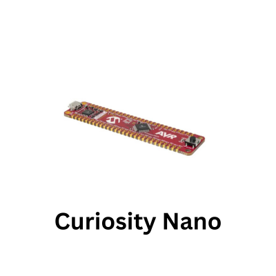
The PIC18F56Q71 Curiosity Nano provides a compact development platform for experimenting with the PIC18-Q71 family without requiring a separate programmer or debugger. The board contains the PIC18F56Q71 itself, an onboard programming and debugging interface, a user-controllable LED, a pushbutton and edge connections that expose the microcontroller pins for external hardware.
This makes it suitable for simple introductory experiments such as controlling an LED, but the same board can also be used to explore the considerably more advanced analog, timing, communication and Core Independent Peripheral features available inside the PIC18F56Q71.
A useful first objective is deliberately modest: create a firmware project, configure one GPIO pin as a digital output and control the board’s yellow LED. That experiment verifies several parts of the development chain at once.
The compiler must recognise the correct device, configuration settings must allow the MCU to execute, the programming interface must communicate with the target, the firmware must manipulate the correct register and the microcontroller must drive the expected physical pin. Once that path is known to work, subsequent experiments with timers, ADCs, UART, SPI, I2C, PWM and the Curiosity Nano Explorer have a known-good starting point.
The PIC18F56Q71 is significantly more capable than the simple LED experiment suggests. It combines conventional digital peripherals with a 12-bit differential ADC with computation, internal operational amplifiers, DACs, analog comparators, configurable logic, programmable signal routing, hardware PWM, Universal Timers, DMA and other peripherals intended to perform useful work with limited CPU intervention.
Understanding the device therefore involves more than learning the instruction set or writing loops in C. A large part of effective PIC18F56Q71 development is understanding how the peripherals can be configured and connected so that hardware performs operations that would otherwise require continual software activity.
Lets look at my hardware setup
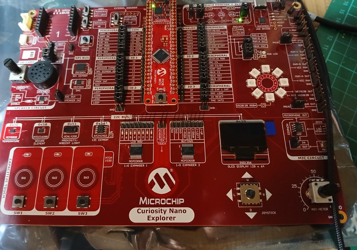
- curiosity setup
The Curiosity Nano Hardware
The PIC18F56Q71 Curiosity Nano contains a 48-pin PIC18F56Q71 together with the circuitry needed to power, program and debug it over USB. For introductory work this removes a substantial amount of setup. There is no requirement to connect an external ICSP programmer simply to load firmware onto the board. The integrated debugger can program the target device and supports normal debugging operations such as breakpoints, stepping through code and examining variables and peripheral registers.
The target microcontroller operates separately from the debugger section even though both occupy the same PCB. This distinction becomes useful when diagnosing unusual behaviour. The debugger is not the application processor; it is supporting hardware that communicates with the PIC18F56Q71. The program being developed runs on the PIC18F56Q71 itself.
Two onboard components are especially useful for the first experiments. The yellow user LED, identified as LED0, is connected to RC7. It is active-low: pulling the associated MCU output low illuminates the LED. Driving the pin high turns it off. This is an important detail because code that assumes an active-high LED appears to behave backwards even though the GPIO configuration is correct.
The onboard mechanical switch, SW0, is connected to RA0. Pressing the switch connects the input to ground. There is no need for an external switch for a basic input experiment, but the input needs a defined idle state. An internal weak pull-up can provide this, allowing RA0 to read high while the switch is released and low while it is pressed.
These assignments are board connections, not general PIC18F56Q71 rules. RC7 is not inherently an LED output and RA0 is not inherently a pushbutton input. They are ordinary MCU pins connected to those components by the Curiosity Nano PCB. This distinction becomes important when the same firmware concepts are moved to a custom PCB.
The board edge connections expose the microcontroller for additional experimentation. Serial interfaces, analog inputs, PWM signals and general GPIO are available through these connections. Many digital peripheral signals on the PIC18F56Q71 can also be routed with Peripheral Pin Select, so the pin shown for a particular serial function should not automatically be interpreted as the only possible pin for that function.
The Curiosity Nano Explorer can be added later when additional hardware is useful. It provides a much richer collection of inputs, outputs and serial devices, including an OLED, LEDs, sensors, controls and communication peripherals. It is not required for the initial LED or switch examples. Using the Curiosity Nano alone initially has an advantage: the electrical path between firmware and physical hardware is easier to understand because fewer components are involved.
Creating a Minimal PIC18F56Q71 Firmware Project
A basic project needs to target the PIC18F56Q71 explicitly. Device selection matters because the compiler’s device header defines the available registers, bit fields, memory layout and other hardware-specific symbols. Code written against a different PIC18 device may compile differently, refer to unavailable registers or configure a peripheral incorrectly even if the devices appear closely related.
A typical C program begins by including the device support header:
#include <xc.h>
#include <stdint.h>
#include <stdbool.h>
With XC8, <xc.h> selects the correct device-specific definitions according to the configured project target. Register names such as TRISC, LATC and ANSELC can then be accessed directly.
The exact oscillator and configuration-bit setup depends on the chosen project configuration. These settings should not be treated as boilerplate that can be copied blindly between projects. Clock configuration affects virtually every time-dependent peripheral. A program may successfully blink an LED with an inaccurate delay while UART baud rate, PWM frequency, timer periods and ADC timing are all wrong because the code assumes a different oscillator frequency from the one actually supplying the CPU.
For a first GPIO experiment, absolute timing accuracy is not particularly important. A delay of approximately half a second is visually distinguishable from one of approximately one second. Nevertheless, it is useful to establish the project clock correctly from the beginning so later peripherals are built on a known frequency.
The PIC18F56Q71 supports a high-frequency internal oscillator and can operate at system frequencies up to 64 MHz when configured appropriately. The application should define its expected oscillator frequency consistently with the actual clock configuration when compiler delay functions depend on that definition.
For example:
#define _XTAL_FREQ 64000000UL
This line does not configure the oscillator. It tells compiler support routines what frequency the application expects. Setting _XTAL_FREQ to 64 MHz while the hardware is actually running at another frequency does not make the MCU run at 64 MHz. It merely causes timing routines based on the macro to calculate delays from the wrong assumption.
That distinction is worth retaining throughout PIC development: a software definition describing hardware state is not necessarily the register configuration that creates that hardware state.
Understanding PIC18F56Q71 GPIO
Digital GPIO on the PIC18F56Q71 uses several register groups that separate pin direction, output data, input state and analog functionality. Four of the most important concepts are represented by TRISx, LATx, PORTx and ANSELx.
TRISx controls direction. A bit set to 1 configures the corresponding pin as an input. A bit cleared to 0 configures it as an output.
LATx is the output latch. When a pin is configured as a digital output, software normally writes the desired output state to the appropriate LATx bit.
PORTx reflects the logic level seen at the port pins. It is therefore particularly important for input operations.
ANSELx determines whether pins capable of analog operation are configured for analog or digital use. This register is frequently overlooked when moving between analog and digital experiments. A pin configured for analog operation may not behave as expected when software tries to use its digital input circuitry.
This separation also explains why experienced PIC firmware commonly modifies LATx rather than writing output changes through PORTx. The latch represents the intended output state, whereas reading PORTx observes the actual pin. Using the appropriate register reduces the possibility of read-modify-write behaviour producing an unexpected result when several outputs on a port are manipulated.
For the onboard LED, the relevant physical signal is RC7, so the direction bit is TRISC7 and the output latch bit is LATC7.
A minimal initialization sequence can therefore look like:
static void LED_Initialize(void)
{
    ANSELCbits.ANSELC7 = 0;
    LATCbits.LATC7 = 1;
    TRISCbits.TRISC7 = 0;
}
The first operation ensures that the pin is being treated as a digital signal where applicable. The second writes a high level to the output latch, which keeps the active-low LED off. The final statement changes the pin direction to output.
Writing the desired latch state before changing the pin into an output is a useful general practice. It means that when the output driver becomes active, the output already contains its intended initial state. This can prevent brief unwanted transitions when a pin controls hardware more consequential than an indicator LED.
LED control functions can then express the active-low behaviour clearly:
static void LED_On(void)
{
    LATCbits.LATC7 = 0;
}

static void LED_Off(void)
{
    LATCbits.LATC7 = 1;
}

static void LED_Toggle(void)
{
    LATCbits.LATC7 ^= 1;
}
Naming the operations according to their physical effect makes the rest of the program easier to read. The main program does not need to remember repeatedly that zero means on.
An LED Blink Test
With the device configured to run at the expected clock frequency, a minimal application can initialize the LED and toggle it periodically.
#include <xc.h>
#include <stdint.h>
#include <stdbool.h>

#define _XTAL_FREQ 64000000UL

static void LED_Initialize(void)
{
    ANSELCbits.ANSELC7 = 0;
    LATCbits.LATC7 = 1;
    TRISCbits.TRISC7 = 0;
}

static void LED_Toggle(void)
{
    LATCbits.LATC7 ^= 1;
}

void main(void)
{
    LED_Initialize();

    while (1)
    {
        LED_Toggle();
        __delay_ms(500);
    }
}
The configuration-bit declarations and oscillator setup used by the surrounding project must correspond to the intended 64 MHz operation. They are intentionally not replaced here with a generic block copied from another PIC18 project because those settings should match the actual project configuration.
The logic itself is straightforward. LED_Initialize() establishes a known high state and then enables the output driver on RC7. The infinite loop toggles the output latch and waits approximately 500 ms. Because one toggle changes the LED from off to on and the next changes it back, a complete visible on/off cycle occupies approximately one second.
The delay is blocking. During __delay_ms(500), the CPU is effectively occupied with producing the delay rather than carrying out other application work. This is entirely reasonable for a first hardware test. It is not an architecture that should automatically be carried into larger applications.
A later timer tutorial can produce the same blink rate using a hardware timer. That allows the CPU to perform other work between LED transitions and introduces a pattern that scales much better when several independent operations must happen at different rates.
Testing the Result on the Board
After programming, the yellow LED0 on the Curiosity Nano should alternate between illuminated and extinguished states at a clearly visible rate. If the software delay corresponds to the assumed clock, each state should last about 500 ms.
This visual result proves more than just LED operation. It demonstrates that the firmware has reached main(), the main loop continues executing, the code is addressing the correct port, RC7 is configured as an output and the physical LED circuit is functional.
If the LED never changes state , better to find where the chain breaks than simply rewrite the program .
A debugger breakpoint at the beginning of main() verifies that the application starts. A second breakpoint inside the loop confirms repeated execution. The TRISC, LATC and ANSELC registers can then be inspected while halted. If TRISC7 remains configured as an input, the problem is in initialization. If LATC7 changes but the physical LED does not, the investigation moves closer to the hardware.
The active-low connection is another common source of confusion. LATC7 = 0 should illuminate the onboard LED and LATC7 = 1 should extinguish it. An application that labels these states the other way around can appear logically inverted while the electrical behaviour is completely correct.
A multimeter is usually unnecessary for this particular experiment because the LED itself provides a perfectly adequate indicator. For less visible GPIO signals, measuring the output pin relative to ground can confirm whether the microcontroller is producing a low or high voltage. A logic analyser or oscilloscope becomes useful when timing must be verified more precisely.
For example, if RC7 is accessible without creating contention with the onboard LED connection, observing the output with an oscilloscope would show a square waveform whose high and low intervals are each close to 500 ms. The waveform period would therefore be close to one second. That measurement also provides an indirect check that the software’s clock assumption is reasonable.
Reading the Onboard Pushbutton
Once an output is working, the next useful GPIO experiment is the onboard switch. SW0 is connected to RA0, and pressing it connects the pin to ground. Because there is no external pull-up dedicated to the switch, the MCU’s weak pull-up can establish the released state.
The input should first be configured for digital operation and input direction. The weak pull-up is then enabled according to the device’s port configuration.
Conceptually, the electrical behaviour is:
Released: RA0 pulled high
Pressed:  RA0 connected to GND
The software interpretation is therefore active-low just like the LED, although for a different electrical reason.
A button helper function might ultimately expose the physical meaning instead of forcing the application to work with raw zero and one states:
static bool Button_IsPressed(void)
{
    return (PORTAbits.RA0 == 0);
}
The remaining initialization must configure the pin as a digital input and enable the appropriate weak pull-up. It is important to use the PIC18F56Q71 register definitions associated with the chosen compiler rather than copying pull-up control code from an older PIC family.
Once configured, the LED can follow the switch:
while (1)
{
    if (Button_IsPressed())
    {
        LED_On();
    }
    else
    {
        LED_Off();
    }
}
This simple relationship introduces input sampling, active-low signals and the difference between reading PORTA and writing LATC.
Mechanical switches also have bounce. Typically a physical button does not go from high to low once and stay electrically perfect. Its contacts can make some rapid transitions when closing or opening. If the program just turns an LED on or off depending on the current level, bounce may not be very obvious. When a person presses a counter or selects a menu option, one physical action may be perceived as multiple presses.
That makes switch debouncing a useful subsequent experiment rather than something that needs to complicate the first GPIO test.
Moving Beyond Delays
The LED program demonstrates GPIO but does not demonstrate an efficient real-time firmware architecture. The half-second delay prevents the main loop from doing useful work during most of its execution time.
A slightly larger application might need to read a pushbutton, refresh an OLED, sample an ADC, process serial input and blink a status LED simultaneously. Giving each task a large blocking delay quickly makes the system unresponsive.
The PIC18F56Q71 includes timer and event resources that can be used to schedule these activities without keeping the CPU inside delay loops. A hardware timer can generate a periodic event every millisecond, ten milliseconds, hundred milliseconds or another selected interval. Software can use that event to update time counters or set flags.
A common arrangement is:
volatile bool led_update = false;
A timer interrupt periodically changes the flag:
void Timer_ISR(void)
{
    led_update = true;

    /* Clear the actual timer interrupt flag here. */
}
The main loop performs the larger operation:
while (1)
{
    if (led_update)
    {
        led_update = false;
        LED_Toggle();
    }

    /* Other application work can execute here. */
}
The exact timer registers and interrupt code depend on which PIC18F56Q71 timer is selected. Those details are best handled in a dedicated timer example where the clock path, prescaler, period calculation, interrupt flag and resulting frequency can all be shown correctly.
The important architectural change is that the CPU is no longer deliberately prevented from executing useful code for hundreds of milliseconds.
Why the PIC18F56Q71 Becomes More Interesting After GPIO
The PIC18F56Q71 includes a substantial collection of peripherals intended to reduce the amount of continuous CPU processing required in embedded designs. GPIO is therefore only the entry point.
Its ADC subsystem, for example, goes beyond taking a single analog sample and returning a binary number. The device provides a 12-bit differential ADC with computation capabilities and multiple contexts. Depending on the required measurement, hardware can participate in accumulation, averaging, filtering and threshold-related operations. This provides a useful path from a simple potentiometer-reading experiment into hardware-assisted signal acquisition.
The integrated operational amplifiers allow some analog conditioning functions to be implemented without placing a separate op amp beside the microcontroller. Combined with the DACs, comparators and ADC, this makes the device particularly interesting for analog measurement tutorials. Rather than connecting every sensor directly to an ADC pin and correcting everything in software, the signal path can sometimes be conditioned and evaluated within the MCU’s analog peripheral system.
Peripheral Pin Select provides similar flexibility on the digital side. UART, SPI and other digital peripheral signals are not simply tied permanently to one arbitrary group of pins. PPS allows supported digital peripheral functions to be assigned to permitted I/O routes. This can simplify PCB layout and allows the firmware configuration to match the hardware design rather than forcing every project into one fixed pin arrangement.
PPS also creates a distinctive failure mode. A UART may be internally configured correctly, generate the correct baud timing and place characters into its transmit register, yet produce nothing on the expected external pin because the transmit output has not been mapped correctly. Understanding internal peripheral configuration and external signal routing as separate steps makes these problems much easier to diagnose.
The Configurable Logic Cells provide another direction. A CLC can combine internal or external digital signals using hardware logic instead of repeatedly sampling those signals in software. Logical functions, gating, latching and peripheral interconnections can therefore be implemented with predictable hardware timing and minimal CPU activity.
The Numerically Controlled Oscillator is useful when programmable frequency generation is required. Instead of relying only on a conventional timer divider relationship, an accumulator-based frequency generator allows fine control over output frequency from an input clock. This makes it a worthwhile progression after basic timers and PWM.
The PIC18F56Q71 also includes DMA channels. DMA allows data movement to occur without the CPU explicitly copying each item. This becomes increasingly useful in applications involving repeated peripheral transfers or data acquisition.
These features are why an effective learning sequence should not remain at the level of LED blink variations for very long. GPIO establishes the register model and hardware workflow, but the device becomes considerably more interesting when several peripherals are allowed to cooperate.
Working with the Curiosity Nano Explorer
The Curiosity Nano Explorer extends the development board into a larger experimental platform. For the PIC18F56Q71 it creates opportunities to exercise both digital and analog peripherals without repeatedly assembling an entire circuit on a breadboard.
The OLED is an obvious early peripheral because successful operation requires several embedded concepts at once. The MCU must initialize the appropriate communication peripheral, route or select the required signals correctly, communicate according to the display controller’s protocol and maintain display data in a suitable format. Once basic communication works, character generation, numeric display, sensor values and small status interfaces can be added.
The Explorer also contains inputs that are useful for ADC experiments. Rather than viewing the ADC only as a peripheral that returns numbers, the application can read a varying input, convert the result to a voltage or scaled engineering value and display it on the OLED. That creates a complete path from physical stimulus to analog acquisition, numerical processing and human-readable output.
Serial peripherals on the Explorer provide another natural progression. I2C experiments can start by establishing bus communication and identifying devices, then move into reading actual sensor registers. SPI can be treated similarly, with attention paid to clock polarity, phase, chip select and signal routing rather than hiding the interface behind a library call.
The value of the Explorer increases when it is used to expose the microcontroller’s peripherals rather than merely as a collection of ready-made components. A temperature sensor tutorial, for example, can be primarily an I2C tutorial. An OLED status display can demonstrate formatted numeric output and bus scheduling. A speaker experiment can lead into timer or PWM generation. A potentiometer can become an ADC acquisition and filtering exercise.
Debugging Register-Level Firmware
Register-level programming makes peripheral behaviour visible, but it also means that initialization mistakes are exposed directly. This is useful educationally because the reason a peripheral works or fails can often be traced to a small number of register states.
When a program fails, debugging should begin with the simplest test that distinguishes between possible causes.
For GPIO, inspect the direction register, analog-select state and output latch. For a digital input, inspect the physical PORTx level while manually changing the input. For UART, verify the clock assumption, baud generator configuration and PPS route before investigating higher-level communication logic. For PWM, verify that the peripheral itself is running and that its output has been routed to the intended pin. For ADC, confirm that the channel and analog configuration are correct before blaming the conversion mathematics.
The onboard debugger is particularly valuable because register values can be inspected while the program is halted. A peripheral that appears mysterious from source code often becomes straightforward once its actual control and status registers are examined.
There is one limitation to remember: halting the CPU can alter the timing relationship between software and active hardware. Breakpoints are excellent for initialization and state inspection, but they are less appropriate when measuring a continuously timed protocol. GPIO timing markers and external test equipment are often more useful for those cases.
A spare output pin can be toggled around a piece of code:
LATBbits.LATB0 = 1;

/* Code being measured */

LATBbits.LATB0 = 0;
An oscilloscope or logic analyser can then measure the width of the resulting pulse. This turns software execution into an observable hardware signal and is a useful technique when investigating interrupt latency, processing time or periodic scheduling.
Serial diagnostic output is another option once UART operation is established. Short textual messages can expose state without stopping the MCU, although excessive printing can itself alter program timing. Instrumentation should therefore be chosen according to the problem rather than added automatically.
Common Problems in the First Projects
One of the easiest mistakes is selecting the right physical pin but leaving its direction incorrect. If TRISC7 remains an input, changing LATC7 does not produce the expected driven output. Inspecting TRISC immediately identifies the problem.
Analog configuration creates a similar issue on pins that support both analog and digital functions. If an input does not respond digitally, ANSELx should be among the first registers inspected.
Another common mistake is expecting PORTx and LATx to serve exactly the same purpose. Reading a port is appropriate when software wants the actual pin state. Manipulating output state should normally use the latch. Keeping those roles distinct reduces subtle read-modify-write problems as applications become larger.
Incorrect clock assumptions can remain hidden during simple experiments. An LED still blinks even if a nominal 500 ms delay lasts noticeably longer or shorter. The error becomes much more serious when the same clock value is used to calculate UART baud rate or PWM frequency. Establishing the actual clock configuration early avoids later diagnostic confusion.
PPS errors become important as soon as peripheral outputs are involved. Configuring a UART, PWM or other peripheral does not necessarily guarantee that its signal appears on the connector expected by the application. The internal peripheral and the external route should be treated as two parts of the configuration.
Copied register code is another recurring source of errors. The PIC18 family spans many generations, and code written for another PIC18 is not automatically correct for the PIC18F56Q71. Peripheral names, available modes, PPS behaviour, analog architecture and interrupt handling can differ. Device-specific register definitions should therefore be treated as part of the design rather than incidental syntax.
Configuration bits deserve similar care. A project may compile perfectly while failing before useful application code is reached because oscillator, reset or other device-level configuration does not match the intended setup. When debugging a completely inactive application, verifying that main() is reached is more informative than immediately changing the GPIO logic.
